ASML: the $380 Million machine you've never heard of

Every iPhone you've ever owned. Every Nvidia chip powering the AI revolution. Every advanced processor in every laptop, server, and data center on the planet.
They all pass through one small Dutch town called Veldhoven.
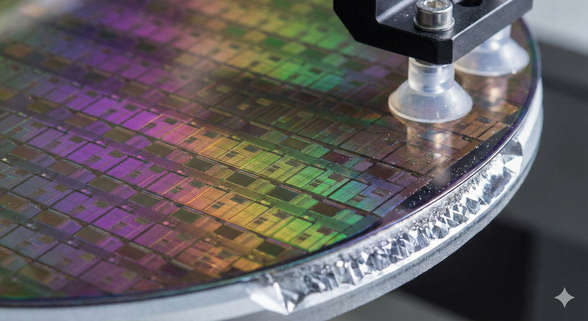
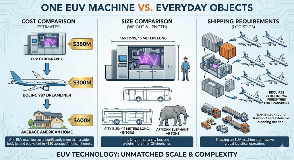
There, a company most people have never heard of builds machines so complex they require seven Boeing 747 cargo planes just to ship (and they require specialized containers that manage temperature, vibration, and pressure). Each one costs $380 million. And ASML is the only company on Earth that can make them.
The silent monopoly behind your screen
ASML has a market cap north of $550 billion. That makes it Europe's most valuable technology company - bigger than SAP, bigger than Spotify, bigger than any European tech firm you could name.
Yet most people couldn't tell you what ASML does if their Netflix subscription depended on it.
The short version: ASML makes the machines that make the chips that make everything else possible. Without ASML, there are no smartphones. No AI. No modern computers. No advanced weapons systems. Nothing that requires a cutting-edge semiconductor.
The company has 100% market share in extreme ultraviolet lithography - the technology required to manufacture the world's most advanced chips. Its only "competitors," Nikon and Canon, are stuck making older-generation equipment that can't produce anything close to modern processors. In the entire history of capitalism, few companies have achieved such complete dominance over technology this critical.
What ASML actually does (without the jargon)
Semiconductors - the chips in your phone, laptop, and car - are essentially billions of tiny circuits printed onto silicon wafers. The smaller you can make those circuits, the more powerful the chip. Three things happen simultaneously as transistors shrink: they get faster, they consume less power, and they become cheaper per unit of performance. That relationship is the engine behind everything from cheaper smartphones to more capable AI models.
The problem? Modern circuits are so small that the width of a human hair would look like a highway next to them. We're talking about features measured in nanometers - billionths of a meter.
You can't print something that small with normal light. The wavelength is simply too long. It's like trying to paint a miniature portrait using a mop.
ASML's solution: extreme ultraviolet light, or EUV.
EUV lithography uses light with a wavelength of just 13.5 nanometers - about 40 times shorter than the light in a standard chipmaking machine. This allows manufacturers to print circuits so small that a single chip can contain over 100 billion transistors.
But generating and controlling this light is absurdly difficult. EUV light is absorbed by air, glass, and pretty much everything else. The entire process has to happen in a near-perfect vacuum. And because EUV light can't pass through lenses, the machine uses a series of mirrors - crafted by German optics specialist Carl Zeiss - polished to sub-atomic smoothness. If one of those mirrors were scaled up to the size of Germany, the largest imperfection would be less than a millimeter high.
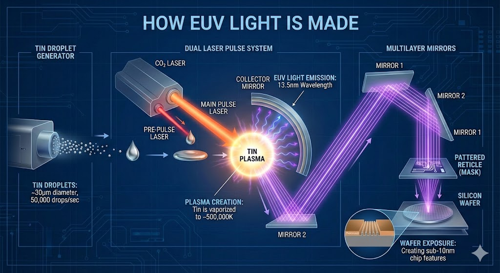
To generate the light itself, ASML's machines fire a high-powered CO2 laser at tiny droplets of molten tin - each about 30 micrometers across - up to 50,000 times per second. A first pulse flattens each droplet into a disk. A second pulse vaporizes it into a plasma hotter than the surface of the sun, which emits the precious 13.5-nanometer light. The physics involved is so extreme that for decades, many experts thought commercial EUV lithography was impossible.
Fun fact: The energy efficiency of this process is almost comically bad. According to ASML's former CTO Martin van den Brink, the machine draws 1.5 megawatts from the electrical grid - enough to power a small neighborhood - but only about 1 watt of EUV light actually reaches the wafer. The rest is lost as heat at every stage of the optical chain. It's the most expensive light on Earth.
The precision required is equally absurd. Cleanrooms where these machines operate must be virtually particle-free. Intel once experienced mysterious nightly drops in chip yield at one of its fabs. After months of investigation, engineers traced the problem to methane from nearby dairy farms drifting into the cleanroom ventilation when the wind changed direction around 1–2 a.m. Cow farts were ruining microprocessors.
Pheeew. Now that we got the tech jargon out of the way, let's go back to business.
The 30-Year bet that created a monopoly
ASML didn't become a monopoly overnight. The company spent three decades and over €6 billion in R&D to develop EUV technology - the longest and most expensive gamble in semiconductor history.
The story begins in 1984, in a leaky shed next to a Philips office in Eindhoven, Netherlands. Electronics giant Philips and chip-machine maker ASM International launched a joint venture called ASM Lithography. The company started with a handful of employees and modest ambitions. Those early years were rough. The semiconductor industry already had established players - Nikon and Canon dominated - and ASML was the scrappy underdog. In 1992, the company nearly went bankrupt, surviving only through a 36-million-guilder emergency loan from Philips.
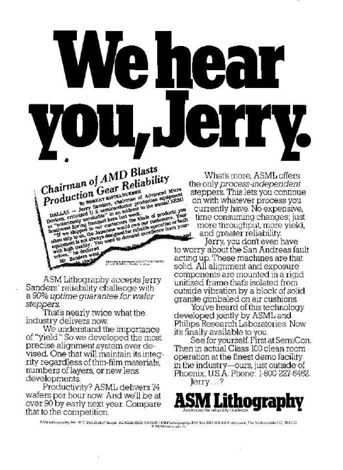
Fun fact: In 1985, when ASML was still a nobody, AMD's CEO Jerry Sanders publicly complained about Japanese machine unreliability. ASML ran a cheeky ad with the headline "We hear you, Jerry" - and bluffed their way into a high-stakes equipment competition they weren't remotely qualified for. They got a meeting. Then they got a customer.
What ASML did differently from day one was counterintuitive. As Marc Hijink documents in Focus: The World of ASML, while Japanese competitors built machines that arrived fully tuned and "plug-and-play," ASML shipped machines that weren't yet perfect. Customers could start their own testing and optimization immediately. By the time a competitor delivered a polished machine, ASML's customer had already fine-tuned their production yield. It was the "perfect enough" strategy - and it worked.
A critical inflection point came in the early 2000s. The industry was approaching the limits of 193-nanometer DUV lithography. Nikon and Canon had invested billions in developing 157-nanometer "dry" tools - the obvious next step. But TSMC's Burn-Jeng Lin proposed an alternative: 193-nanometer immersion lithography, using water between the lens and the wafer to shorten the effective wavelength. While Japanese firms hesitated, ASML and TSMC partnered to commercialize immersion tools by 2004. This single decision rendered billions in Japanese R&D obsolete and allowed ASML to capture 70% of the lithography market by 2009.
But the real gamble was EUV. In the late 1990s, ASML joined a US consortium including Lawrence Livermore and Sandia National Laboratories to explore the foundational science. By 2006, they shipped their first EUV prototype. It produced one wafer in 23 hours. For context, a modern chip factory needs hundreds of wafers per hour to be economically viable. One wafer in 23 hours was a curiosity, not a business.
By 2012, the R&D costs threatened to overwhelm even ASML. In what insiders called the "Musketeer Project," ASML convinced its three largest customers - Intel, TSMC, and Samsung - to buy equity stakes and co-fund EUV development. Intel alone committed €829 million to R&D and acquired 15% of the company. These direct competitors became collaborative partners, sharing the financial risk of a technology they all desperately needed to exist. It was a co-opetition model virtually unique in industrial history.
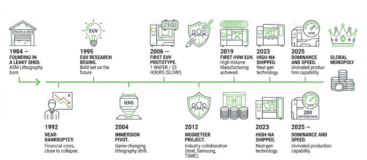
Today, an ASML EUV scanner produces up to 200 wafers per hour - a 4,600x improvement from that first prototype. The company has now shipped its next-generation High-NA systems, which use a wider numerical aperture (0.55 vs. 0.33) to print features at just 8 nanometers. These machines weigh 165 tons, cost up to $400 million each, and require seven Boeing 747 cargo planes to transport. Once they arrive, 250 engineers spend six months assembling and calibrating them. The 30-year bet didn't just pay off - it created an entirely new era of atomic-scale manufacturing that the industry is calling the "Angstrom Era."
The numbers that explain everything
ASML's 2025 financial results tell the story of a company operating at a scale most businesses can't comprehend.
Revenue hit €32.7 billion, up 16% from 2024. Net income reached €9.6 billion. The order backlog stands at €38.8 billion - enough orders to keep factories busy through 2027. Gross margin: 52.8%. In Q4 2025 alone, the company booked €13.2 billion in new orders, a quarterly record.
But the truly staggering numbers are in the machines themselves. Each contains over 100,000 individual parts - rising to 450,000 in the High-NA laser systems - sourced from nearly 800 suppliers across the globe. The optical system alone, made by Zeiss, requires mirrors polished to a smoothness where any imperfection larger than a few atoms would ruin the machine.
ASML shipped 48 EUV systems in 2025 and 300 total lithography systems. At $200–400 million per EUV unit, the math is straightforward. Revenue is concentrated among a handful of customers: TSMC, Samsung, SK Hynix, Intel, and Micron. Order lead times stretch 18 to 24 months - the longest in the semiconductor supply chain - giving ASML an extraordinary window of revenue visibility that most cyclical tech companies can only dream of.
For 2026, ASML projects revenue of €34-39 billion. The long-term target: €44-60 billion by 2030. Already, the company is proposing "Hyper-NA" tools - with a numerical aperture of 0.75 or higher - expected to cost upwards of $724 million each and enable chips at the 0.5-nanometer node by the early 2030s.
Why nobody can compete
At this point, you might wonder: if EUV machines are so valuable, why doesn't someone else make them?
The answer reveals one of the most fascinating competitive moats in modern capitalism - and it's built on four reinforcing pillars.
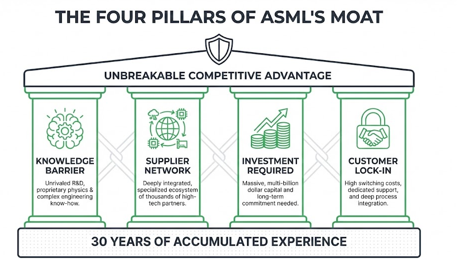
The knowledge barrier. ASML spent 30 years developing EUV through trial and error, encountering thousands of dead ends. Even if a competitor had unlimited funding, they'd face an insurmountable problem: you can't compress 30 years of institutional learning. The Silicon Triangle report calls this "tacit knowledge" - the unwritten expertise held by engineers that exists in neurons, not in filing cabinets. ASML holds over 16,000 patents, but the real moat is the millions of lines of proprietary code and decades of calibration data that no blueprint can capture.
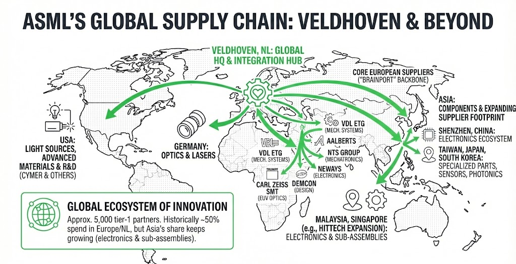
The supplier network. ASML doesn't build most of the machine itself - it produces roughly 15% of the components in-house and acts as a "systems architect" for an ecosystem of over 5,000 specialized suppliers. The most critical is Zeiss, which makes the optical systems. As Hijink describes it, this isn't a traditional vendor relationship - it's a "two companies, one business" symbiosis built over 25 years. ASML holds a 24.9% stake in the Zeiss subsidiary. The same deep integration extends to Trumpf (the laser supplier) and dozens of others. A competitor wouldn't just have to build a better machine - they'd have to build a better Zeiss and a better Trumpf. Those companies don't exist.
Fun fact: The ASML-Zeiss bond runs so deep it even extends to patent warfare. When Nikon sued ASML for patent infringement, ASML and Zeiss struck back by acquiring digital camera patents and announcing the Zeiss ZX1 - a consumer camera almost certainly built as a legal weapon rather than a real product. The camera proved Nikon was infringing on their IP, and Nikon settled.
The investment required. EUV development cost over €6 billion in R&D alone, part of a total industry investment estimated between $14 and $21 billion. ASML continues to spend nearly €5 billion annually on R&D - about 14% of revenue. This creates a feedback loop: ASML owns 83% of the total lithography market, and the massive cash flow from this position funds the next generation, making it impossible for newcomers to catch up. As the Fabless authors describe it, this is the semiconductor industry's version of a "learning curve" moat - competitive advantage driven by accumulated experience that reduces costs 20-30% with every doubling of production volume.
Customer lock-in. ASML's customers have built their entire manufacturing processes around its machines. Their fabs are designed for ASML's equipment. Their engineers are trained on ASML's systems. Their process recipes assume ASML's specifications. Each EUV machine typically comes with its own embedded ASML technician who remains on-site for the tool's 30-year life. Switching to a hypothetical competitor would require retooling entire factories worth billions of dollars.
ASML's monopoly isn't the result of anti-competitive behavior. It's the result of being the only company persistent enough to spend three decades solving a problem everyone else thought was impossible.
The geopolitics of light
ASML's monopoly has made it the most geopolitically significant company most people have never heard of. Both the United States and China desperately need access to ASML's machines - and both are willing to reshape global trade policy to get (or block) them.
Why China can't catch up. China has poured over $180 billion into developing domestic semiconductor manufacturing. But without access to EUV machines, Chinese fabs are stuck producing chips that are generations behind the cutting edge. ASML has never sold an EUV machine to China, and thanks to export controls, it likely never will. In December 2025, Reuters reported that China has secretly assembled an experimental EUV-like scanner - codenamed "Wuxie" - but experts expect it won't produce viable chips before 2028-2030 at the earliest. ASML's CEO has been blunt about the odds: "The laws of physics in China are the same as here."
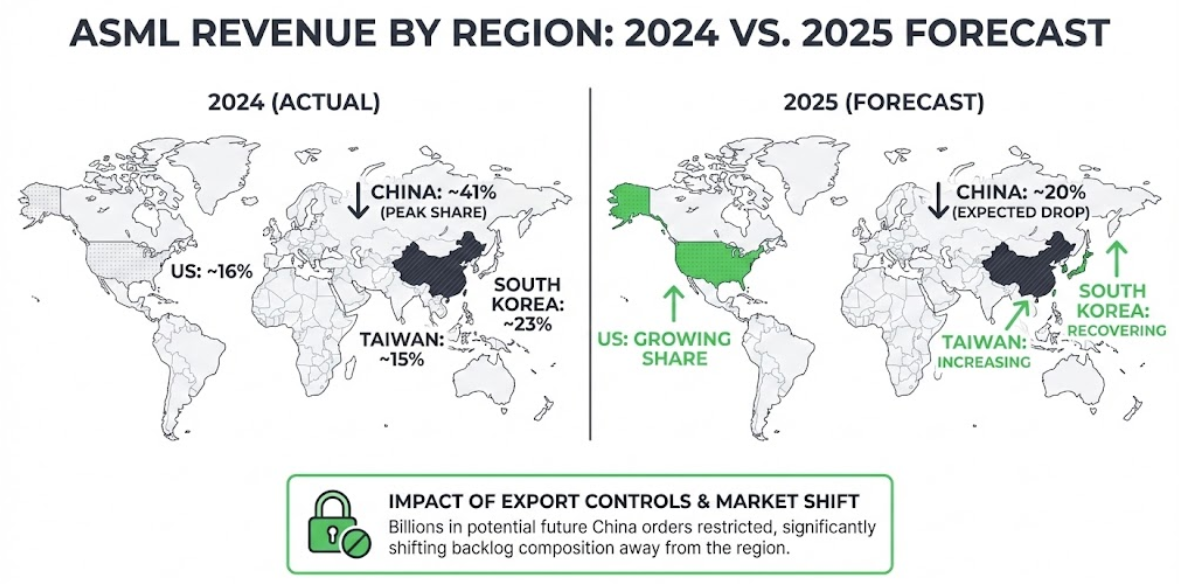
The export control escalation. In 2019, the US worked with the Dutch government to block EUV sales to China. But the controls have expanded dramatically since then. By late 2024, even ASML's older DUV immersion machines were restricted. In January 2026, the Trump administration added 25% Section 232 tariffs on AI-related semiconductor equipment and introduced a "revenue sharing" fee for export licenses. The impact on ASML has been dramatic: China accounted for 49% of ASML's revenue in 2024 as Chinese customers frantically stockpiled machines before bans took effect. By 2025, that figure dropped to approximately 20%.
But there's a twist that few investors appreciate. As Hijink argues in Focus, this decoupling is a double-edged sword. Cutting off Chinese revenue doesn't just slow China - it removes a massive revenue source that ASML needs to fund its own next-generation R&D. Without that cash flow, the investment cycle for Hyper-NA and future technologies could slow down, potentially shrinking the very technological lead the export controls were designed to protect.
China's counter-punch. China hasn't taken the restrictions quietly. In 2025, Beijing began restricting exports of rare earth elements used in semiconductor manufacturing equipment - a direct response to the lithography bans. And the Silicon Triangle authors warn of an even more potent long-term strategy: while the West obsesses over cutting-edge 3nm chips, China is quietly moving to dominate "mature node" chips at 28nm and above - the ones in every car, appliance, and medical device. By subsidizing these older chips, China could flood global markets, destroy Western profit margins, and gain the same chokepoint leverage it holds over rare earths.
Europe's accidental leverage. The most critical chokepoint in the US-China tech war isn't controlled by either superpower. It's controlled by a Dutch company in a town of 45,000 people. ASML's former CEO Peter Wennink once characterized the Netherlands as a "Mickey Mouse country" caught between superpowers, trying to stay above the geopolitical fray. But as Hijink documents, the company eventually learned that "America sets the rules" in the new Silicon Curtain era. Dutch export policy now shapes the future of Chinese AI development, American military technology, and the global balance of power.
What this means for you
You're probably not in the market for a $380 million lithography machine. But ASML's story has real implications for anyone interested in technology, investing, or understanding how the modern economy actually works.
For understanding modern technology. Every headline about AI, every announcement about the latest smartphone chip, every story about semiconductor shortages - they all trace back to lithography. When TSMC announces a new 3-nanometer chip, they're talking about circuits printed by ASML machines. When Nvidia can't meet demand for AI chips, production bottlenecks often involve lithography. Understanding ASML means understanding the foundation on which the entire digital economy is built.
For understanding geopolitics. The US-China tech war isn't really about apps or social media. It's about who controls the ability to manufacture advanced semiconductors. The Silicon Triangle authors frame this through the lens of "Value Creation vs. Value Capture" - inventing a technology means nothing if you can't manufacture it at scale. ASML is the ultimate example: the US invented much of the underlying EUV science at its national labs, but it's a Dutch company that captured the value by spending 30 years industrializing it.
For evaluating investments. ASML is one of the clearest examples of what Warren Buffett would call an "economic moat" - and studying it reveals what to look for in any moat company. The strongest moats aren't built on a single advantage. They're built on reinforcing layers: technological exclusivity, supplier lock-in, cumulative R&D, and massive switching costs - all feeding each other. When you evaluate any company as a potential investment, ask the ASML questions: Could a competitor with unlimited money replicate this in 10 years? Are the customers locked in by infrastructure, not just preference? Does the company's current revenue fund the R&D that widens the moat for the next generation?
ASML passes all three tests. Its order backlog extends to 2027. Revenue is projected to grow to €34-39 billion in 2026, with long-term targets of €44-60 billion by 2030. But no moat is permanent. Geopolitical tensions could disrupt supply chains. Export controls have already cost billions in Chinese sales. And eventually, some future technology - perhaps Hyper-NA's successor, or a paradigm shift away from photolithography entirely - might reshape the landscape. The strongest moat in the world is still subject to the passage of time.
The unlikely champion
ASML's story is the opposite of the typical tech narrative.
No garage startup mythology. No hoodie-wearing founder disrupting incumbents. No growth hacking or viral loops or network effects. Instead: a 40-year-old Dutch company that spent three decades solving an engineering problem everyone said couldn't be solved, using technology so complex that even after 30 years, nobody else can replicate it.
Fun fact: When ASML went public in 1995, the IPO instantly created 40 millionaires among its employees. True to Dutch Calvinist culture, almost none of them flaunted it. The spending stayed modest, the focus stayed on yield. As Hijink writes, in ASML's culture, showing off wealth is considered bad manners - and a distraction from the mission.
Europe doesn't produce many global technology leaders. It's lost the social media wars, the search engine wars, the smartphone wars. But in lithography - the technology that makes all other technology possible - Europe has achieved something neither superpower can match.
The most important machines in the world are built by 44,000 employees in a small Dutch town, using components from 5,000 suppliers across 60 countries, assembled with knowledge accumulated over three decades of relentless engineering.
And every chip that powers the AI revolution, every processor in every phone and laptop and server, still has to pass through their hands first.